
2016
- Incorporation
- Developed "High Power EDFA" 2W prototype
HiPA Photonics Pte. Ltd. was established in 2010 and located in the confluent area of semiconductor industry companies in Singapore. HiPA is a high-tech company supported by the Singapore Economic Development Board.
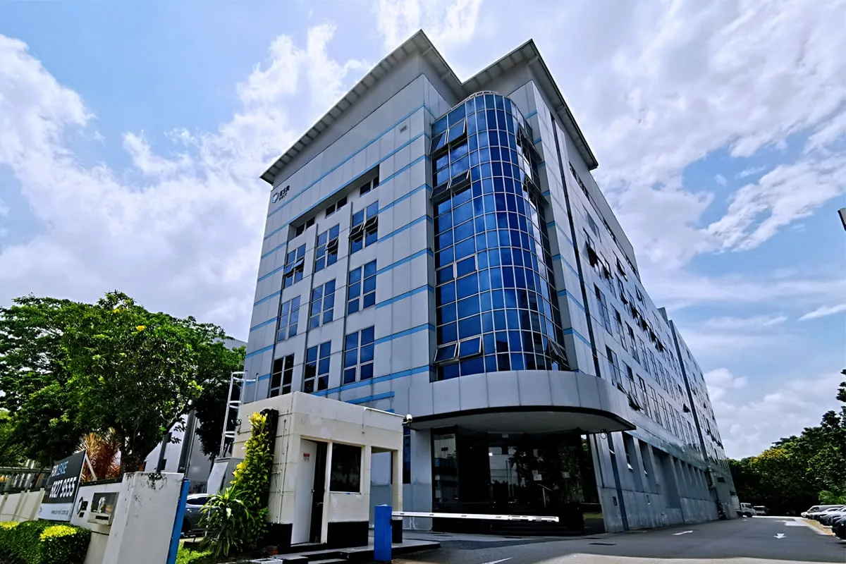
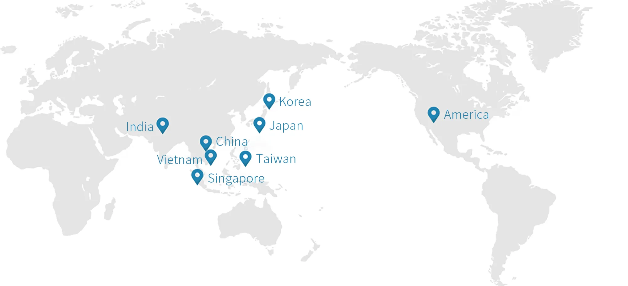
HiPA Photonics Pte. Ltd. was established in 2010 and located in the confluent area of semiconductor industry companies in Singapore. HiPA is a high-tech company supported by the Singapore Economic Development Board. It covers an area of 30160.73 sqft, gathering Nanyang Technological University, National University of Singapore and other well-known universities at home and abroad, it has more than 300 senior R&D talents, who have conducted in-depth research in the fields of new energy, automobile, special materials, semiconductor, passive devices, and consumer electronics, HiPA consists of four product lines: Chip Resister Product Line, Module Tester Product Line, Welding & Joining Product Line, and Advance Laser Product Line. With customers in 27 countries/regions around the world, HiPA is long-term partner with world-renowned technology brands. HiPA has branches and offices in China, the United States, Japan, South Korea, India, Vietnam and other places. Its Huizhou production base has a total construction area of over 17500 square meters.
Since its establishment, HiPA focuses on cutting-edge research and unremitting endeavors in high precision automated optical inspection and laser micro-processing integrated equipment. The measurement results of HiPA equipment are benchmarked against the US NIST (National Institute of Standards and Technology), which is highly accurate and recognized world-wide. On the basis of high precision, HiPA perfectly integrates advanced optical technologies with automation technologies in a bid to produce high-precision and high-performance intelligent equipment. HiPA not only successfully helps customers to greatly improve their quality inspection accuracy, production efficiency, and their economic profit, but also frees countless production workers from the tiredness caused by high-intensity repetitive work and the irreversible injuries caused by long-time naked-eye inspection.
HiPA technology has entered thousands of families along with every micron-sized chip resistor, every microsensor, every high-performance electronic devices and every high-quality display to escort the quality life of people. HiPA, just like the dolphin logo in the trademark, is not only highly intelligent but also friendly and kind, which often saves people out of trouble and brings them safety; though HiPA has held the most advanced technologies, HiPA always serves every customer heart and soul, constantly strives for perfection, and use the highest quality to achieve the peace of mind of end-users.

International R&D team accounted for 30% of total personnel, Doctors 20+, masters 80+,600+ national patents
International leading technologies, extremely high precision. NIST traceable measurement results. Fully customized as required
Professional and comprehensive technical support to ensure all aspects of equipment
Respond promptly within 24 hours, technical support covers everywhere in the world
Comprehensive solutions, seamlessly connected parts, and highly integrated systems; rigorous and efficient quality control system, high utilization of feeded materials, and effectively reduce material waste and production cost
High Precision & Accuracy
Make perfection more perfect, Be considerate at every micron
Drive light with intelligence, Measure exactness, Machine perfection

• Ph.D, NTU, Singapore
• Part-time Associate Professor of Wuhan National Laboratory for Optoelectronics
• Senior Member of Institute of Electrical and Electronics Engineers (IEEE), Chairman of Guangdong IEEE
• Member of Chinese Optical Society of Laser Processing Committee
• International Conference Best Paper Award in SPIE 2007
• Type-A Grants of “Peacock Plan” for Overseas High-level Innovation Talents in Shenzhen


• B.Eng (1st Honors), Ph.D Valedictorian, NTU, Singapore
• 3 International Conference Best Paper Awards: ICOCN (2017), OFSIS (2017), OGC (2016)
• Type-C Grants of “Peacock Plan” for Overseas High-level Innovation Talents in Shenzhen


20 years sales experience
Accumulate excellent sales resources for the company
Establish a complete sales system
Quickly occupy the market and win high recognition from customers
Responsible for business expansion in Asia Pacific


Bachelor of Applied Physics, Shanghai Jiaotong University
Master of Science, Nanyang Technological University, Singapore
Singapore Economic Development Board Scholarship
Engaged in machine vision industry for more than ten years, with rich industry experience
Obtained several patents in key fields at home and abroad

Master of National University of Singapore
Has more than 10 years of system design and development experience
In-depth knowledge of each module of the machine
Responsible for the development of software systems for various smart devices

Degree in EE, UM ,Malaysia
15 years in automation with laser intergration

PhD, NTU, Singapore
Committee member of IEEE Photonics Society Singapore Chapter
Selected for Global Young Scientists Summit 2019

Ph.D. NTHU, Taiwan
Vision and R&D Lead at Humanoid Robot StartUp
MEMS Characterization Staff Engineer at Qualcomm
Associate Researcher and PM at ITRC

Ph.D, NTU, Singapore
More than 8 years of research experience in optical fiber and fiber laser
Organizing committee, CLEO-PR, OECC, PGC conference in Singapore, 2017

Ph.D, NUS, Singapore
‘Top 100 Materials Science papers’ of Scientific Report Journal in 2017

Doctor of Philosophy in Electrical and Electronics Engineering, 2009
Nanyang Technological University, Singapore
– Joined Temasek Laboratories @NTU and initiated a new research direction focusing on photonic analog to digital conversion (ADC)
– Took the role of a Principal Investigator (PI) / Senior Research Scientist at the Nanyang Technological University, leading optoelectronic research program
– Currently leading the team of Optical Engineers in-charge of developing innovation technology and company’s IP in optics and laser integrated systems
Group online marketing developer and administrator
Machine design and technical innovation contributor and projects review
Group IT architecture improvement adviser and ongoing support
Group management staff advisor
Bach of Electrical &Electronics engineering