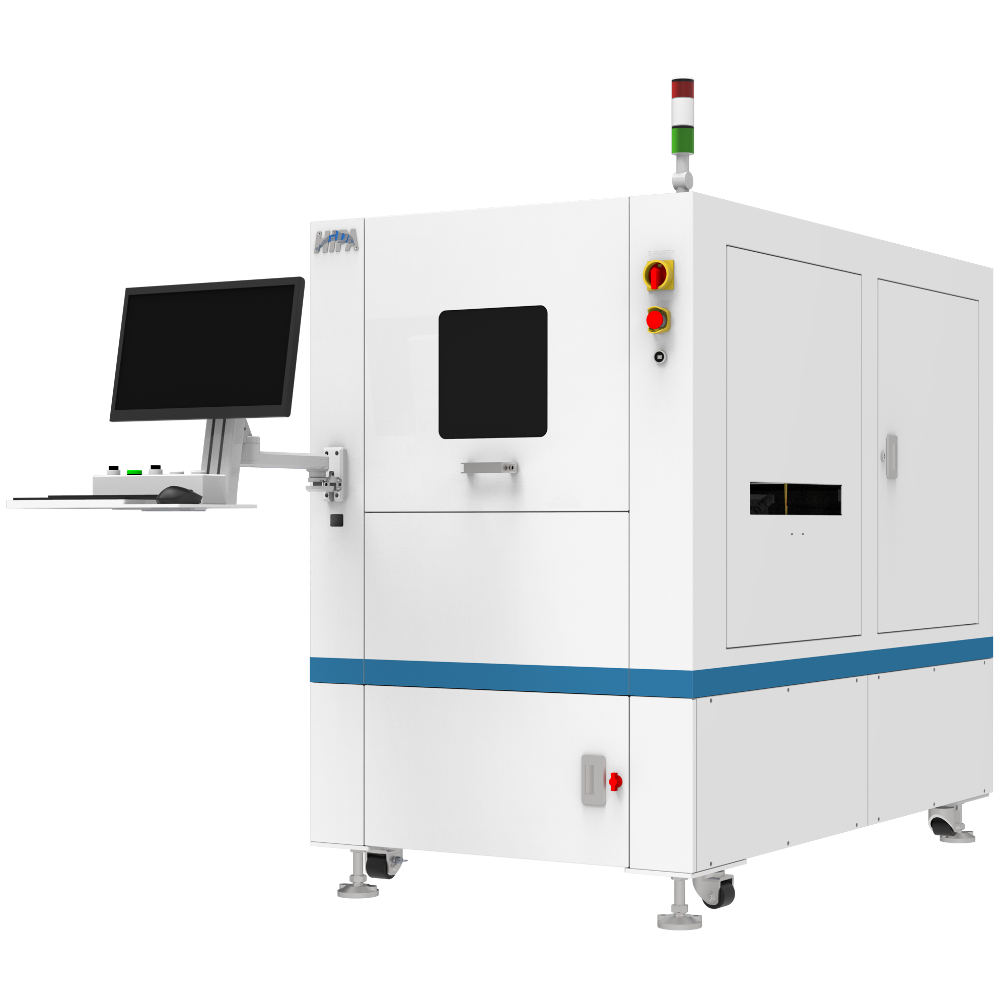
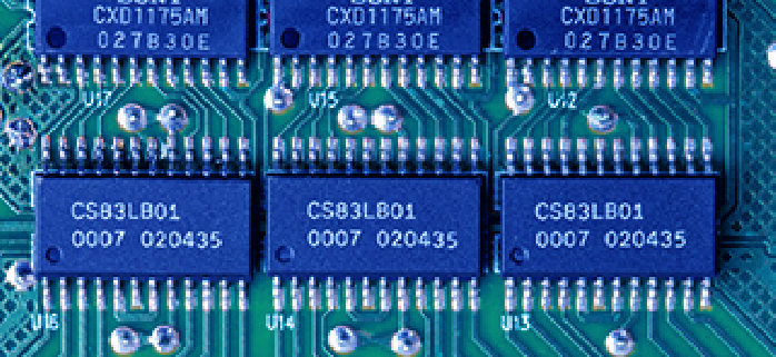
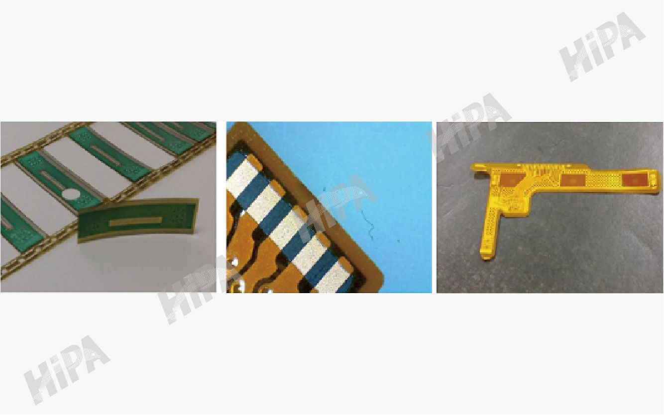
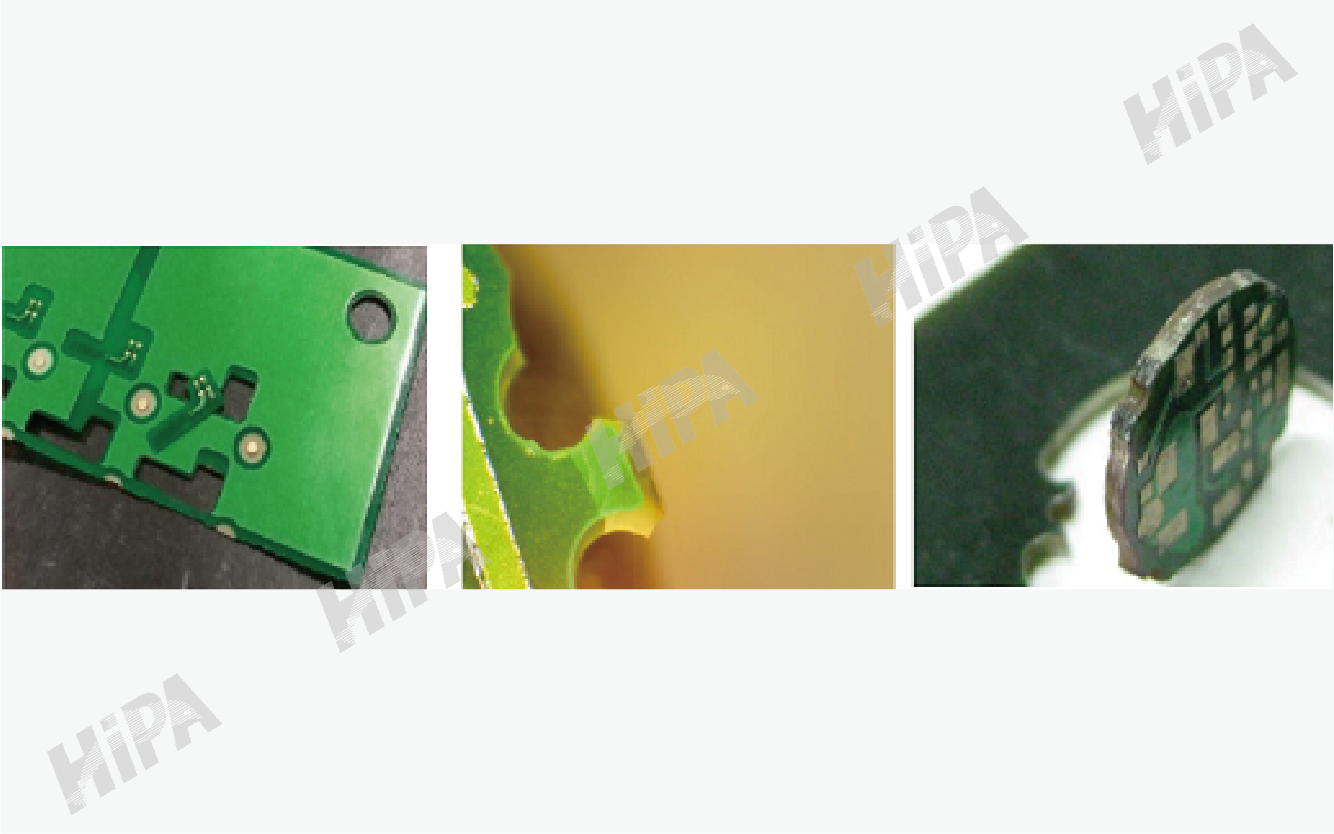
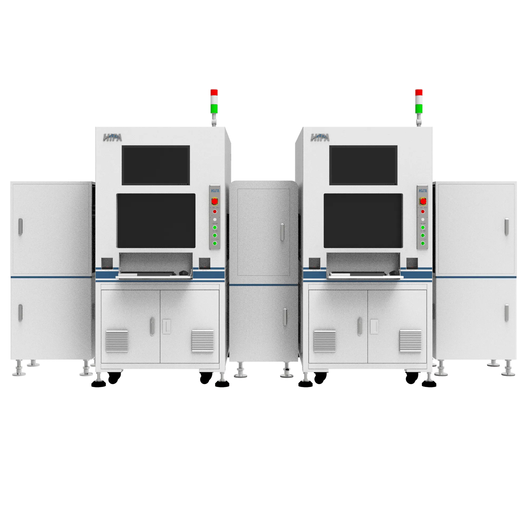
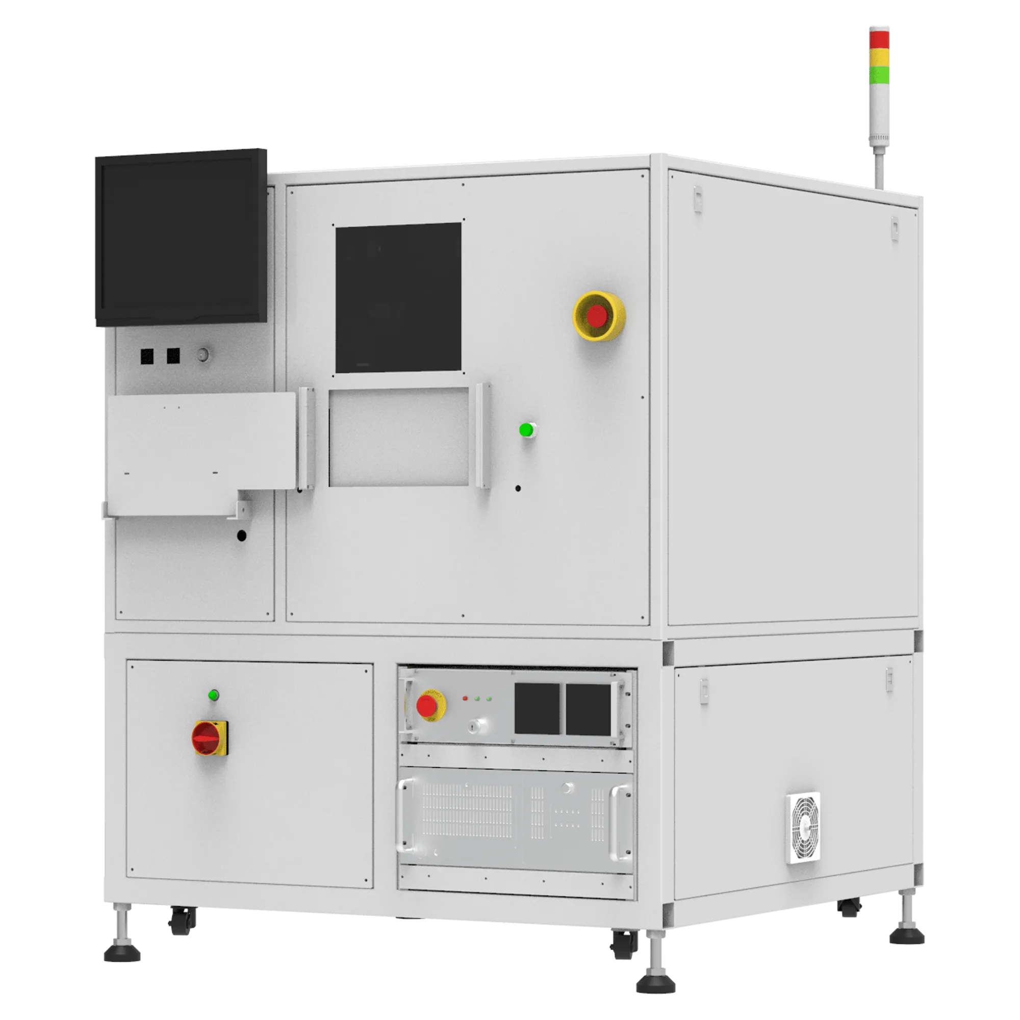
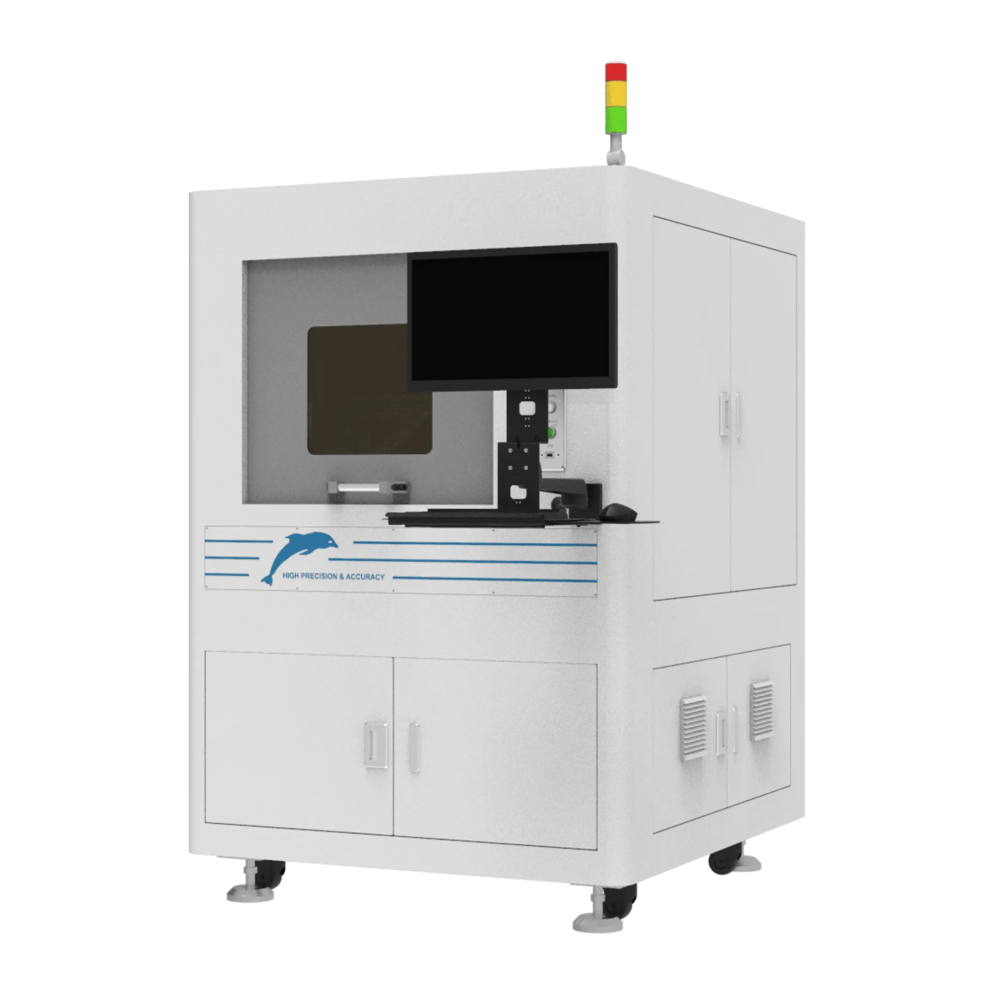
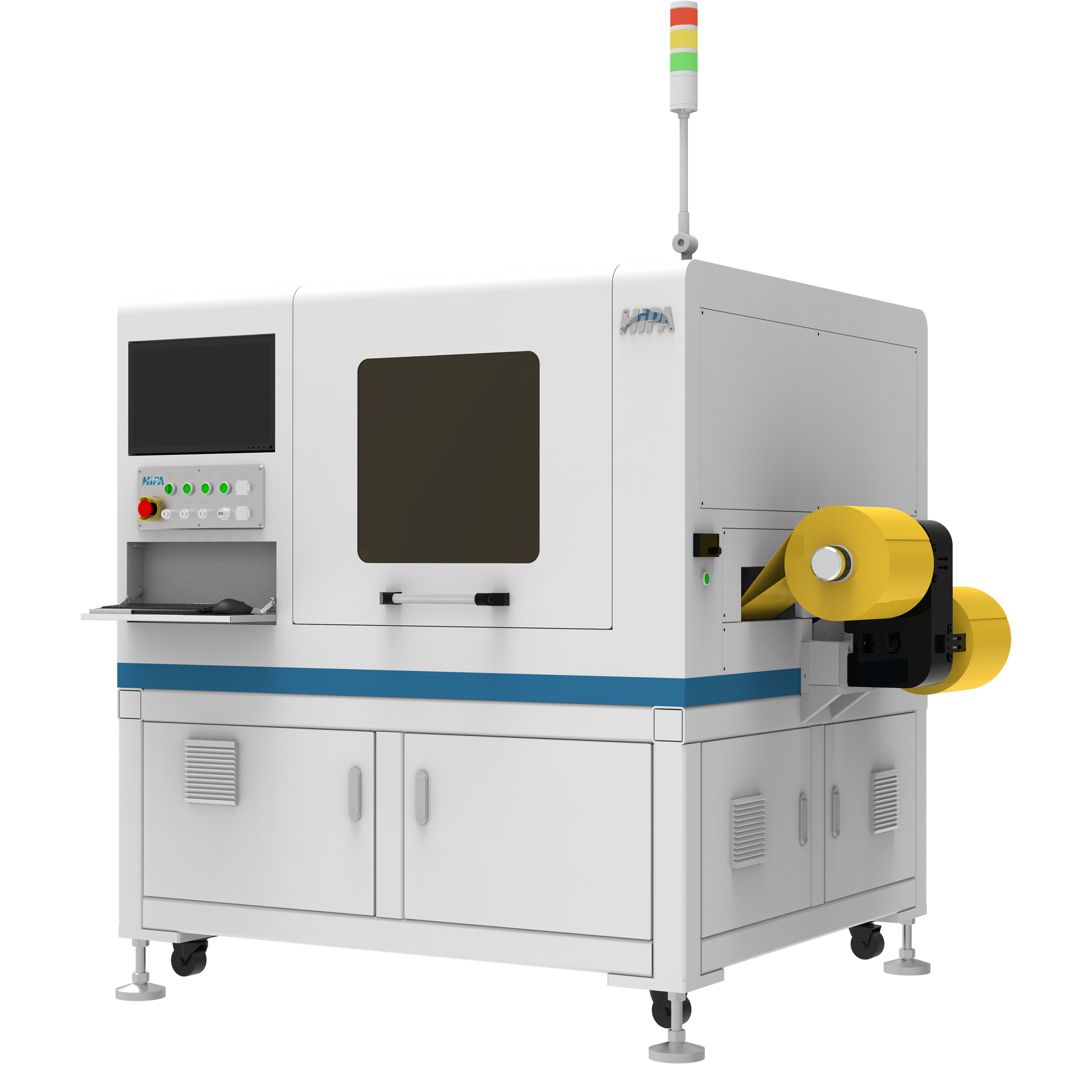
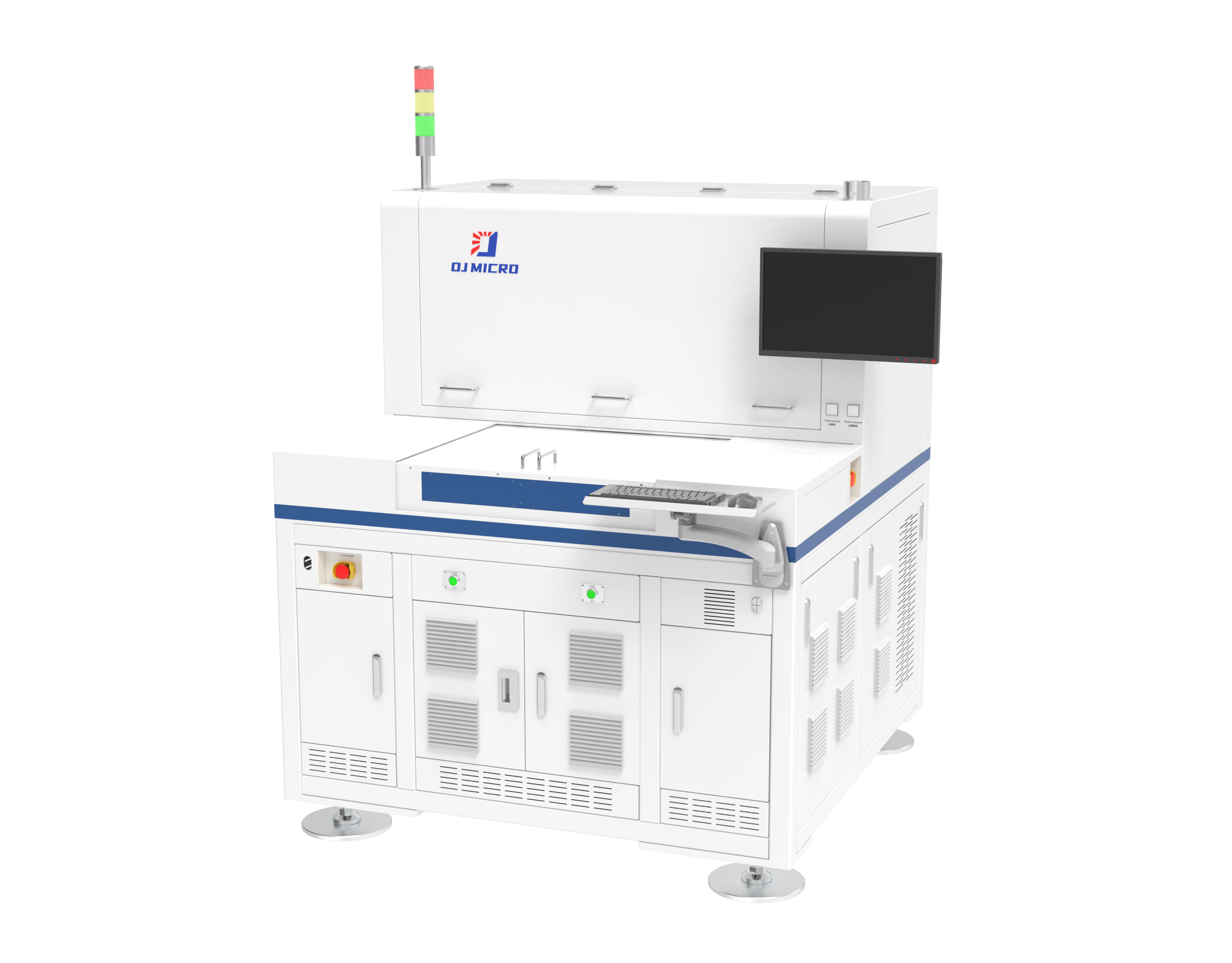
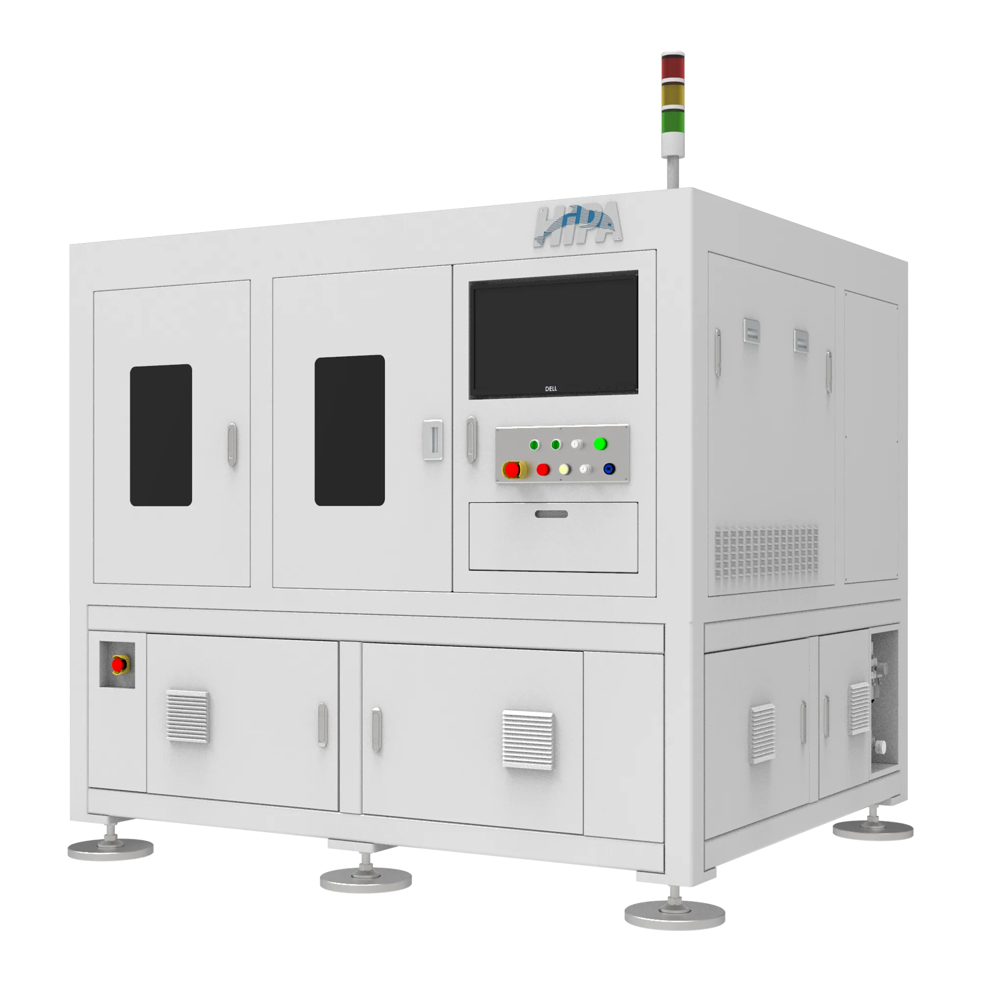
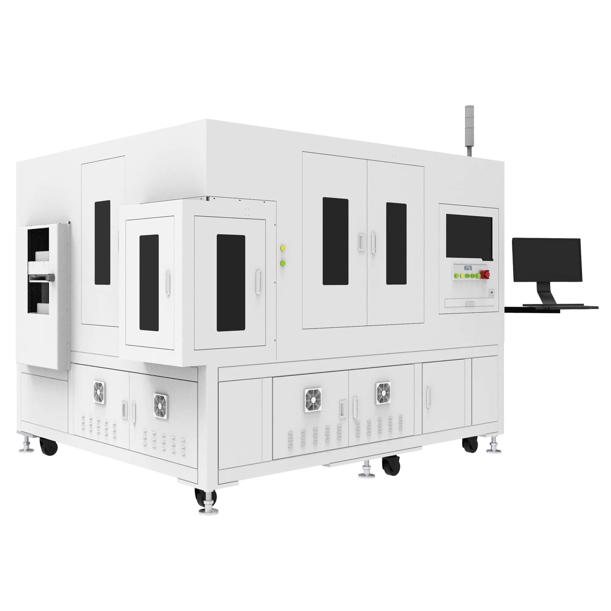
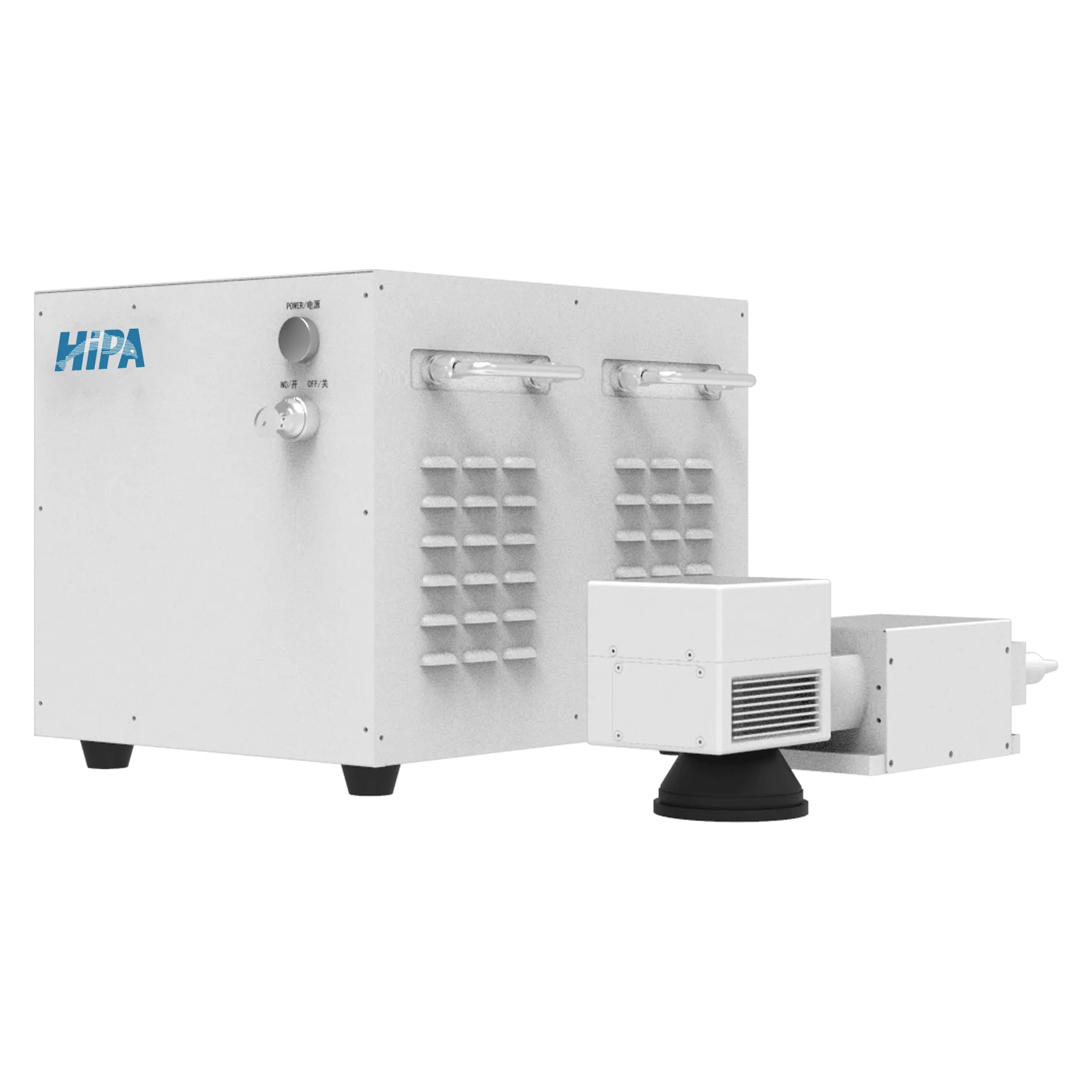
PCB Depaneling is suitable for cutting various types of PCB substrates, such as soft and hard bonding boards, FR4, PCB, FPC, fingerprint recognition modules, covering films, composite materials, copper substrates, aluminum substrates, etc. It can be equipped with ultraviolet or green laser according to needs, and the splitting process is clean and dust-free to avoid circuit failure caused by conductivity caused by waste materials. Help customers solve production efficiency and yield issues. Compatible with products with a maximum size of 460×460mm.
Video
Play Video
Advantages
1. Adopting high-performance lasers, laser cutting has a small heat affected zone and can more effectively process high-density and highly integrated PCB products;
2. Cut the product section without carbonization, blackening, and low thermal impact; Less smoke and dust during the cutting process;
3. Adopting independently developed control software, supporting multiple PCB industry drawing file formats, with functions such as large format product cutting, fast switching between different products, automatic focusing, and compensation for expansion and contraction, meeting the processing requirements of structurally complex products;
4. Adopting high-precision motion systems, scanning mirrors, and visual positioning systems to ensure product processing accuracy;
5. Integrated into the SMT production line and connected to the loading and unloading mechanism, reducing manual intervention and improving production stability.